High Power Medium Frequency and Medium Voltage Dual Active Bridge
Principal Investigator: Dr. Adel Nasiri
Read More:
Wide Band Gap (WBG) power semiconductors, such as Silicon Carbide (SiC) MOSFETs, will have a potentially transformative impact on the power density, efficiency and reliability of Solid State Transformer (SST). High voltage breakdown capability and development of integrate-able MV-rated half-bridge Switch Modules with voltage ratings up to 10kV reduce the number of levels required to implement Medium Voltage (MV) interfacing converters. Today, engineering samples of 15kV rated SiC MOSFETs and 24kV SiC IGBTs have been built and tested in the literature with the possibility of up to 30kV rated devices on the horizon. However, achievement of the same or higher power throughput in WBG-based SSTs, with higher rated devices, is limited by the complex design considerations and trade-offs within the medium frequency transformer design such as switching frequency, dv/dt, core losses, core saturation and inter-winding insulation, winding-to-core insulation and ground-wall insulation. Further complicating the drive towards higher power throughput is the coupling of thermal management into the ground-wall insulation requirements at the system level. The collective impact of these considerations is limiting the reported 13.8kV-connected medium frequency transformer power throughput to levels below 50kVA.
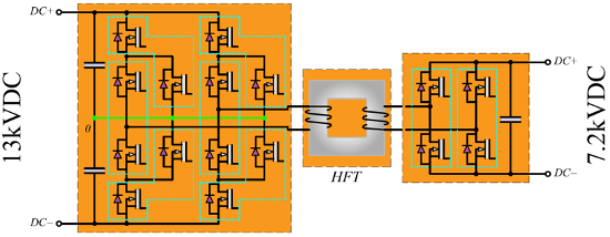
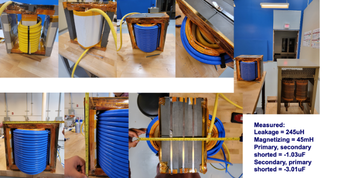
The goal of this project is to develop a Medium Voltage (MV), high power, high frequency dual active bridge as a building block for future MV AC and DC systems. The input voltage is 13kVDC and output voltage is 7.2kV. The power rating is at 667MVA for a 2MVA three-phase system operating at 20kHz. The project pushes the envelope on power and voltage levels for power electronics systems. It has four major tasks: (i) topology development, (ii) controls and modeling, (iii) transformer design and development, and (iv) packaging considering creepage and clearance distances and common mode noise. The controls, modeling, and loss of the entire system has been formulated and conducted. The transformer is designed for appropriate leakage inductance, winding and core insulation, saturation, partial discharge, leakage capacitances, high frequency operation, and thermal management. The H-bridge at the primary is a three-level topology using 10kV SiC MOSFETs. System current for various power transfers has been formulated to achieve minimum RMS and reduced loss. The modeling is performed in ANSYS multi-physics for the H-bridges and transformer.
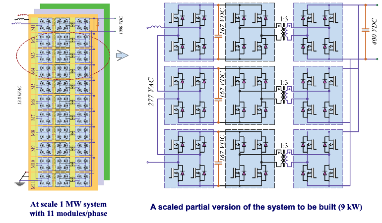
Ultrafast Charging-Development of a compact Direct Medium Voltage Battery Charger
Principal Investigator: Dr. Adel Nasiri
Read More:
Due to the increasing need for low voltage (LV) DC supply for high power applications such as electric vehicle charge station, oil and gas fields, and other electrification needs, studies on medium voltage (MV) AC to low voltage DC converter are required. The main problem in developing these types of converter is lack of commercial availability for efficient medium voltage switches. While Si-based switches cannot generally meet the efficiency and high frequency switching requirements, SiC-based switches are not available above the 1700 V at scale. Therefore, a step down transformer is typically required to reduce the voltage for a DC-DC conversion. An Input Series Output Parallel (ISOP) multilevel structure with an additional DC/DC stage allows using low voltage semiconductor switches at medium voltage level, as well as reducing the EMI and harmonics. Major research needs to develop this topology are development of a high power high frequency transformer and advanced controls to ensure high efficiency.
This proposed converter research project will develop a novel architecture for medium voltage AC to low voltage DC converter offering several improvements over the existing state-of-the-art technologies including compact size, modular structure, scalability to different voltage and power level, and high efficiency. The proposed converter structure is selected as series input parallel output multilevel converter with Dual Active Bridge (DAB). The design will be performed for a 1 MW AC-DC-DC converter. It will have superior advantages such as galvanic isolation with high frequency transformer that will accept 13.8 kVAC medium voltage from the grid and generate direct 1 kVDC to supply loads. To reach 13.8 kVAC voltage level with commercial available SiC switches, 11 modular AC-DC-DC converter structures are required for each phase. Every module power level is planned for 30 kW to a total of 1 MW. Each module has two main stages: AC-DC rectification and DC-DC converter stage. In the first stage, when AC-DC power conversion is performed in unity power factor, a robust control structure is proposed for voltage balancing operation between the modules. In second stage, DAB converter and High Frequency (HF) transformer will be investigated. Although, DAB converters are widely used in power conversion especially Solid State Transformer structure, they have some drawbacks such as circulating current at low power/duty cycle level and high peak current value problems as a result excessive losses at transformer and switches. The proposed algorithm suggests a new RMS current reduction control to reduce losses and to increases the power density. On the other hand, the high frequency transformer design is essential for DAB converter. For this purpose, core material, wire selection and winding placement will be investigated. Due to time and budget constraint, a three level single-phase prototype will be developed instead of 11 levels. 277 VAC input voltage will be converted to 400 VDC voltage level. Each module power will be designed as 3 kW. This will provide the necessary knowledge, expertise, and experience to ultimately develop the three-phase MV converter.
Distributed Energy Resources-Highly Efficient and Compact Medium Voltage Solar PV Inverter
Principal Investigator: Dr. Adel Nasiri
Read More:
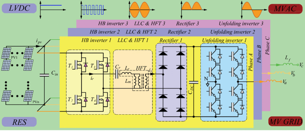
Many studies have been presented on various inverter topologies and control algorithms to obtain high efficient, compact and cost effective inverter designs for grid- connected PV systems. However, these studies are mainly focus on low voltage grid systems. The proposed inverters are usually used with a low frequency transformer (LFT) in order to connect to medium voltage grid. The LFT increases the size, volume and cost and decrease the efficiency of the system. The proposed project will develop a novel inverter architecture for solar PV systems, which enables direct connection of the inverter to the Medium Voltage (MV) grid without any low frequency transformer. The proposed system employs a H-bridge inverter, high frequency transformer (HFT) and full-bridge diode rectifier. The DC-DC converter stage is capable of reaching MV voltage with appropriate transformer turn ratio. In the proposed system the DC-DC converter stage is controlled to generate rectified sine wave voltage and current at the secondary side DC bus. Thus, the inverter employed at the secondary side operates at line frequency and only inverts the rectified sinewave voltage and current to AC. This design and operation at line frequency reduces the grid side transients and improves efficiency. Replacing the LFT with the HFT provides significant improvements in terms of size, volume, cost and efficiency. In addition, by employing LLC resonant converter, which can achieve zero voltage switching (ZVS) and zero current switching (ZCS), in DC-DC converter stage total switching losses can be decreased and the efficiency of the system is increased. The proposed single-phase resonant converter cells operating in buck-boost mode also enables much wider Maximum Power Point Tracking (MPPT) range. In addition, the proposed system is able to provide Volt-VAR support for the electric distribution systems.
In summary, the proposed system provides an unprecedented level of efficiency improvement by using (i) resonant PV side converter operating at zero current switching minimizing switching loss, (ii) using high frequency transformer, reducing the loss significantly compared with low frequency transformer, and (iii) using low frequency unfolding circuitry to practically eliminating the switching loss. The conventional 60Hz transformer creates a continuous power loss in the system even if the solar PV system does not generate any power. The proposed system additionally improves the efficiency by de-energizing the high frequency transformer when there is no power generation.